


When designing RF and microwave circuits, it’s important to take into account a few key design factors. This blog post provides guidelines on how to design RF and microwave circuits using proper design principles and engineering hardware.
By following these guidelines, you can ensure that your circuits are frequency accurate, robust against interference, and fit within your design limits. Keep in mind that the design of RF and microwave circuits is a complex process, so be sure to consult with an experienced engineer if you have any questions. Thanks for reading!
Design Aspects To Consider For Rf And Microwave Pcbs And Assembly
RF and microwave PCB assembly design guidelines are essential for ensuring consistent performance and compliance with FCC regulations. When designing an RF or microwave PCB assembly, it’s important to take into account the intended use and application area.
Guidelines for assembling RF or microwave PCBs include proper soldering techniques as well as accurate alignment of parts during manufacturing. It’s also important to follow applicable quality control procedures in order to ensure consistent performance over time. By following these guidelines, you can ensure that your RF or microwave PCB assembly meets your specific requirements and meets all FCC requirements.
Rf And Microwave Pcb Assembly Requirements
When it comes to embedded system design, quality is always the key. This is especially true when it comes to choosing a supplier – make sure you use someone who has an excellent track record and follows design guidelines carefully. It’s also important to note the physical dimensions of devices when designing circuit boards.
For example, if you are assembling a board that will be used with a handheld device, make sure your layout takes this into account. Failure to do so might result in interference issues between components on the board and the device itself!
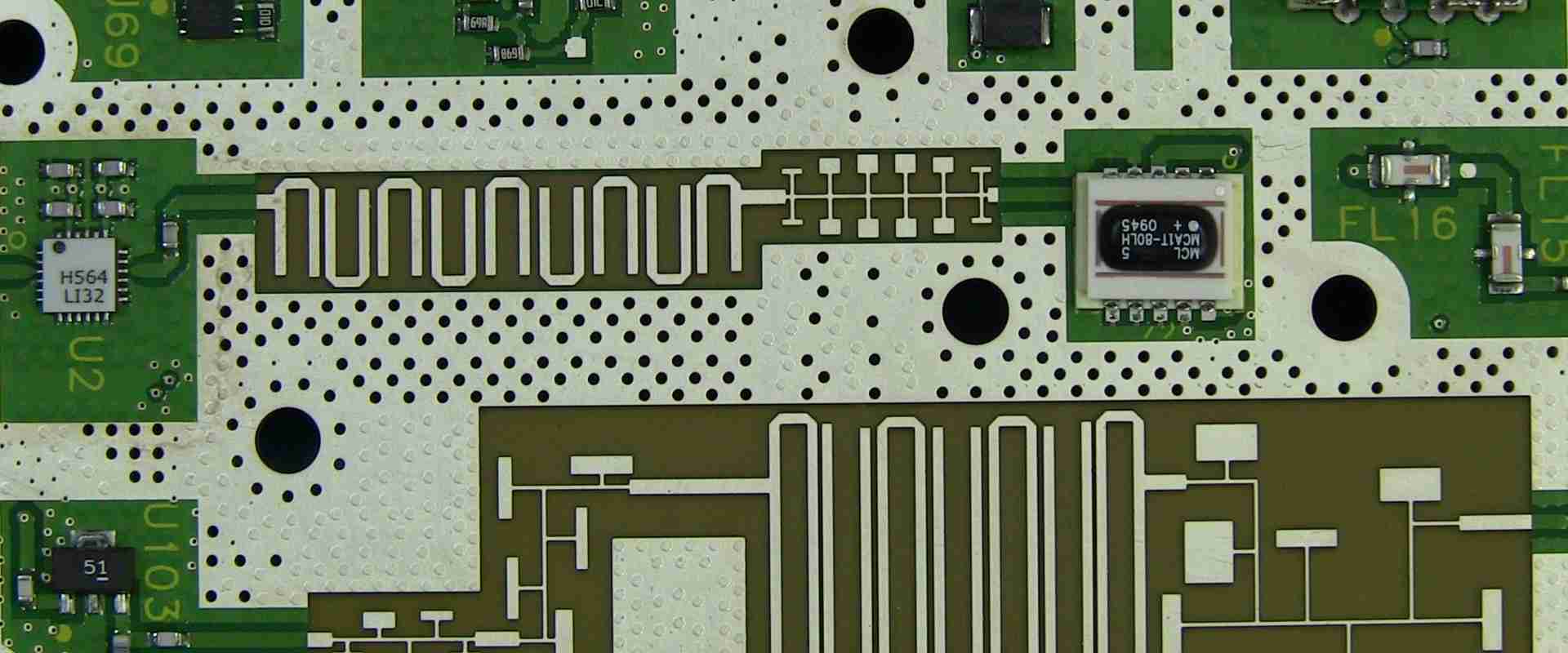
Layout Of Rf And Microwave Components On A Pcb
Layout of RF and microwave components on a PCB is critical for two primary reasons: – It ensures that the signals routed through your board are properly delivered; and – Improper layout can lead to signal loss, poor performance, and even failure.
To help you achieve optimal results when assembling your PCB, we’ve put together some layout guidelines specific to RF and microwave signals. Keep in mind that these rules may vary depending on the frequency range covered by your board – so be sure to consult with a design specialist if you’re not familiar with this topic. Finally, make sure all connection points are properly marked (with trace or via insertions) as well as tested prior to assembly begins. Doing so will help ensure correct signal transmission throughout your circuit boards!
Grounding, Placement And Wiring Off And Microwave Components
When it comes to RF and microwave components, a ground plane is of utmost importance. Poor layout can result in interference and poor performance.
The placement of the components is also critical, as improper assembly will lead to problems with alignment, crosstalk, etc. Wiring should be done properly in order to avoid shorts circuits and other issues that might occur. Ensuring proper grounding also helps optimize circuit performance
Interference Problems With Rf & Microwave Signals
Whilst RF and microwave signals can be very useful, they can also cause interference with other electronic equipment in your building. This can lead to damage to the equipment, loss of data, and even slowed down performance.
To avoid any such problems, it is important that you take into account the design aspects of RF and microwave PCBs when assembling them. You should also follow all relevant safety guidelines while working with these signals.
Guidelines For Screwless Assembly
When it comes to assembling your hardware, make sure you take care in the layout and design of your components. This will help with ensuring correct assembly and less interference between different parts. When screws are necessary, be sure to use the right size and type for the job at hand. And finally, take special care when designing any cavities or holes on your PCBs as they may cause problems down the line.
Choose The Right Materials
When it comes to choosing the right materials for your PCBs, you need to be mindful of the harsh environmental conditions they will be subjected to. For RF and microwave-sensitive products, using a material that is not only resistant but also intended for those environments is essential. Furthermore, make sure you test your boards before assembly in order to avoid any problems down the line.
Choose a quality material that can handle high heat and humidity levels – something not all materials are capable of doing. Follow the guidelines provided when assembling your PCBs for best results – this way, you can rest assured that everything will go smoothly on launch!
Proper Soldering Technique For Rf And Microwave Pcbs
Soldering is an essential step in the assembly of RF and microwave PCBs. Follow proper soldering technique to avoid any potential malfunctions that could result in loss of signal or damage to the circuit boards.
To ensure a safe and successful assembly process, use correct size and type of solder paste, fluxes etcetera. Make sure all connections are made properly – no shorts! Finally, make sure you have a good understanding of how signals pass through electronic components before assembling these circuits board-style.
About Safe Handling Of Rf And Microwave Pcbs
When it comes to the safe handling of RF and microwave PCBs, it is always important to take precautions. Always use a grounded work area – this will help avoid any electric shocks. Keep RF and microwave PCBs away from sources of magnetic fields like computers, speakers etc. Avoid touching the printed circuit boards directly – use gloves or a tool to do so. Always wear protective equipment when handling high voltages and currents.
Tips For Testing And Commissioning Your Board
Testing and commissioning your board is essential for ensuring proper functionality. Here are a few tips to help you along the way:
1. RF (radio frequency) and microwave PCBs are very sensitive to interference, so make sure all electrical components are properly shielded. This will minimize any unwanted noise emissions.
2. The antenna should be placed as far away from the board as possible in order to reduce noise levels generated by it; ideally, it should be mounted on a separate mast or pole altogether!
3 Make sure your assembly is tested before shipping it out – this will help identify any issues right at the start and avoid long-term complications down the line.
Conclusion
Here, we will be discussing design aspects that should be taken into account when designing PCB design board. By following the guidelines outlined, you will ensure that your circuit boards are of high quality and meet all the necessary safety standards. Make sure to read through the blog and learn what you need to know to design RF and microwave PCBs and assemblies that meet your specific needs.


